Inside the Xhorse XT27A Super Chip
Sniffing a VVDI mini programmer as it sets the ID on an Xhorse XT27A super chip, and decoding what it says.
Below is the complete capture of the VVDI mini setting the Type to ID4C and writing UID d3da834c7e39ee98. Blue boxes are what the programmer sends, orange boxes are what the chip answers. Click the graph, then scroll to zoom; drag to pan; the table below lists every message. Zoom in on any box to see the individual bits sitting on the waveform.
Hopefully by the time you have read this post the plot will make sense to you.
Fig. 1 - Sniffed VVDI → XT27A session. Click a box (or a row in the table) for the decoded meaning. Encrypted messages show the ciphertext on the air and the plaintext recovered with the session keystream.
Background
The XT27A or “VVDI super chip” is a programmable rfid transponder chip sold for use with Xhorse car key programming tools. It can be configured to emulate a large number of different transponders. These are the findings of an investigation into the programming protocol to try to add support for these chips to the Proxmark3 so they can be used without buying an Xhorse programmer. All the following information was reverse engineered based on discord chat logs of CastleBravo, HenryGab, klmn, and others investigating the chips’ crypto and the Hitager source by kivijakola https://github.com/kivijakola/hitager
Since it was reversed with Claude’s help there may be errors and mistakes so take this with a pinch of salt. This post is partly for my benefit to document the findings so far and partly to encourage others to look at this and improve our understanding of these chips. The section “How sure am I?” lists what was measured and what was inferred.
The xt27a is configured using a custom version of the HITAG2 protocol, there appear to be 2 variants which I am going to imaginatively name Channel A and Channel B as the Channel B seems to be how the XT37B and XT57B chips are programmed. Channel B has not been investigated beyond its “wakeup string” is XMICRO. The rest of this document is about the xt27a and the Channel A protocol.
Capturing traces
Recordings of the VVDI mini configuring the xt27a chip were made using a proxmark3 and the command lf sniff Initially the Proxmark3 was held over the VVDI mini but later on it was found that placing the VVDI mini on top of the proxmark3 worked.
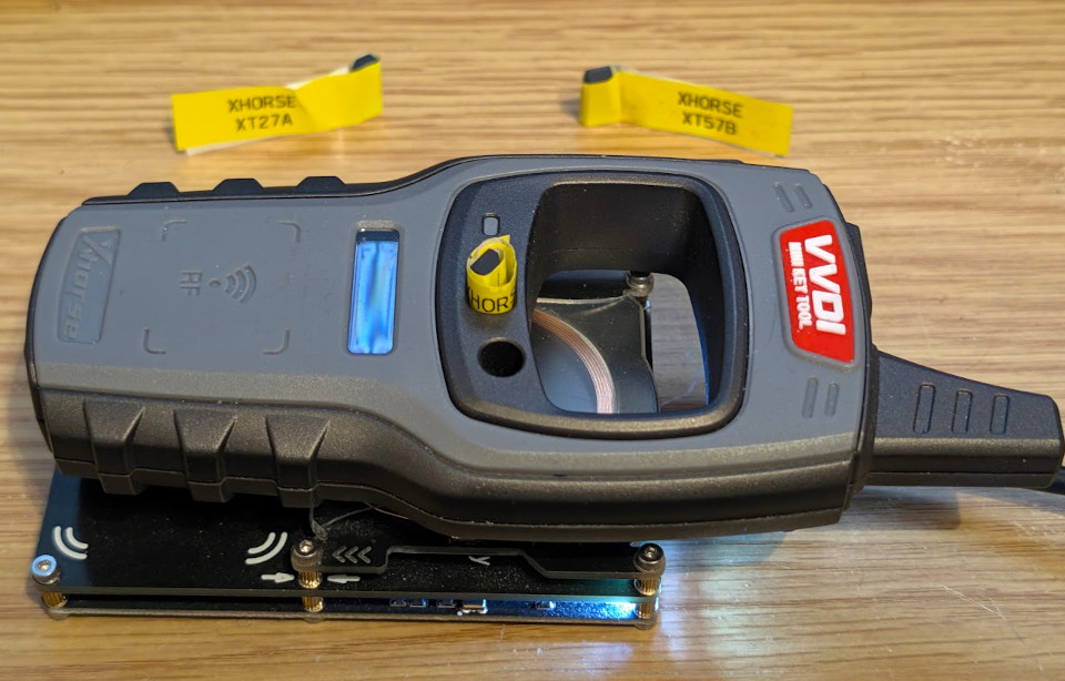 Fig. 2 - The VVDI mini placed on the Proxmark3 for sniffing communications
When you run lf sniff, the Proxmark3 uses its LF antenna to receive the 125 kHz field generated by the VVDI Mini and records the signal as ADC samples. The resulting trace shows the envelope of the signal rather than the carrier waveform itself.
For reader-to-transponder communication, the reader uses BPLM (Binary Pulse Length Modulation) and the transponder answers by load modulation using Manchester encoding (RF/32). These traces were saved as .pm3 files and claude was used to initially write a python decoding script and then to port that to javascript to make the trace visualiser/decoder that is on this page. The visualiser at the top of the page has the example trace used for all the descriptions in this write up but the visualiser below has several different traces you can choose to view, or you can upload your own.
The physical layer
The chip communication is based on the HITAG2 protocol where the reader to chip communication is encoded using Binary Pulse Length Modulation (BPLM). The reader transmits by briefly switching its field off before each bit. The tag only needs to measure how long it was between field restarts.
This is measured in units of T0 which is the carrier period time (1⁄125 kHz= 8 µs). In the plot at the top, message 1 (the XHORSE probe) is a run of these bits: zoom in until the bit cells appear and compare the short and long periods.
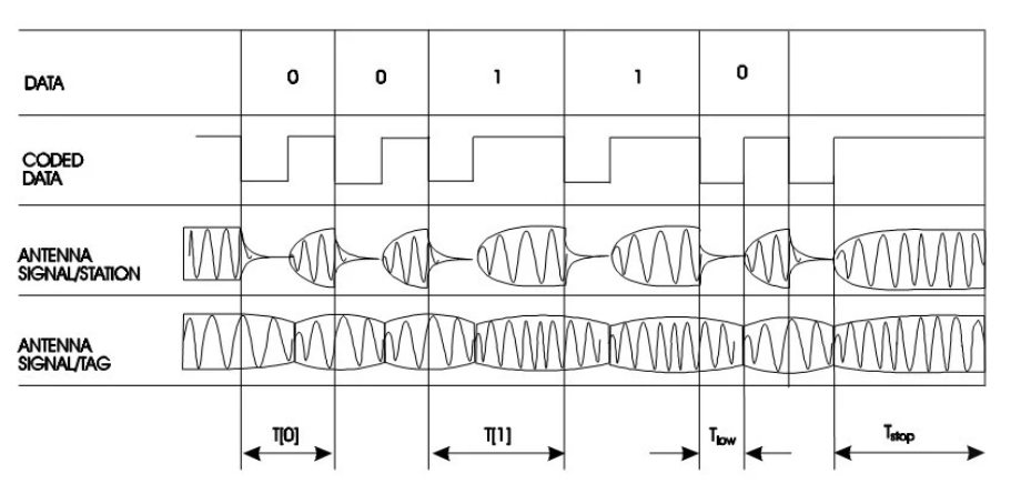
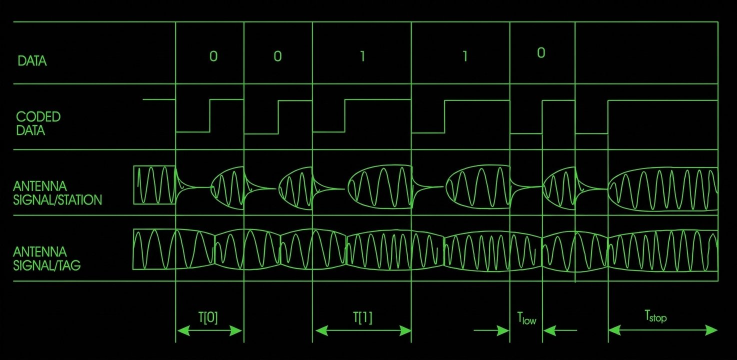 Fig. 3 - BPLM timing from the HITAG2 transponder IC data-sheet, p. 10
| Symbol | Description | Duration |
|---|---|---|
| tlow | low field time | 4..10 T0 |
| T[0] | logic 0 period | 18..22 T0 |
| T[1] | logic 1 period | 26..32 T0 |
| tstop | high field for stop condition | > 36 T0 |
The transponder to reader communication uses Manchester encoding with a bit length of 32 T0 = 256 µs, about 4 kbit/s. Every reply starts with a start of frame (SOF) of five 1 bits (11111), which is not part of the data.
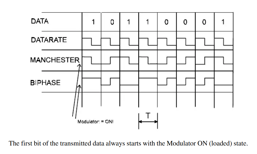
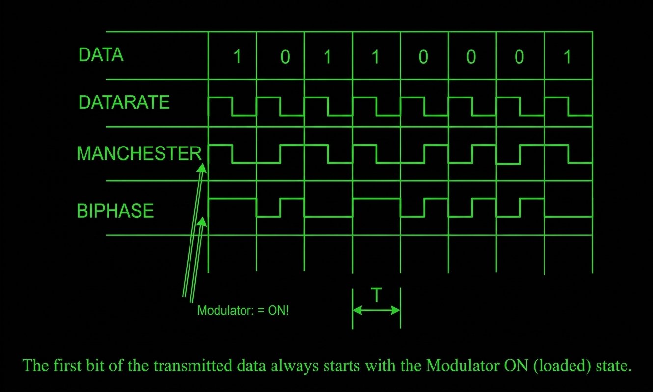 Fig. 4 - Manchester timing from the HITAG2 transponder IC data-sheet, p. 8
Message 2 in the plot is the chip’s reply (0x5AA5): the dimmed cells at the start are the SOF and the rest are Manchester bits (the “Bits” checkbox draws the cells).
Measuring the timing of a VVDI mini, when the chip switches from listening to transmitting (tWAIT1) there is a delay of 193-195 T0 (spec 199-206) and switching from transmitting to listening (tWAIT2) the VVDI mini waits 87-162 T0 (spec min 90) after a reply ends to send its next command.
After a write, the reader waits about 1600 T0 (12.8 ms) before the next command. Presumably this is the chip’s EEPROM write time. You can see it in the plot, between the data of message 15 and the next command (message 16): the gap is 1598 samples.
Channel A: handshake and cipher setup
The reader first sends the ASCII string XMICRO looking for a chip that uses channel B (xt57b) but that is not yet understood so we shall skip that.
A programming session always follows this order:
- The reader sends the ASCII string XHORSE to probe for an xt27a chip, if one is present it will respond with
0x5AA5(message 1 and message 2). - The reader then sends
0x072Fand the tag responds with0xC8F6B638(its meaning is unknown, but it is the same in every capture; message 3 and 4). - The reader then sends
0x7372and the tag responds with a 16 bit value which seems to be a timing counter and is used as the seed for the LFSR. When tested with a delay sweep, the high byte ranges over0x50..0x6B. In every sniffed programming trace it is0x6B, because the official tool uses the same fixed spacing each time (message 5 and 6). The reply is then converted to the LFSR’s starting state:
seed = bitrev16(reply) ^ 0xE12E(For reply =
0x6B3C:bitrev16(0x6B3C) = 0x3CD6, and0x3CD6 ^ 0xE12E = 0xDDF8)
Despite the “auth” naming, nothing secret is exchanged in this handshake: the chip sends the value the seed is derived from in the clear, and the seed formula is fixed. Anyone who hears the exchange can compute the keystream.
1
2
3
4
5
6
7
8
9
10
11
12
13
14
15
16
  reader (VVDI mini)                          chip (XT27A)
-----------------------------------------------------------------------------
"XHORSE"  (48 bits, ASCII)       ------>
                                 <------      0x5AA5                      "I know that word"
0x072F    (16 bits)              ------>
                                 <------      0xC8F6B638 (32 bits)  constant in the captures
      ~11.8 ms gap (fixed in VVDI mini,  determines the value of the seed.)
0x7372    (16 bits)              ------>
                                 <------      0x6B3C     (16 bits)  timing counter = session seed
-------------------------- everything from here on is XORed with the LFSR keystream --------------
0x9C46    (= 41BE ^ ks)          ------>      sel bank 1
                                 <------      0x0E06       echo of the command
0x25F7                           ------>      READ page 0x3F
                                 <------      0xF4F50A5D   (32 bits of encrypted data)
...                                           more sel / WRITE / READ pairs
field off                                    (chip resets)
With the LFSR configured the communications continues with the messages being XOR’d with the output of the LFSR. The first command which was referred to as 4R on the discord is always 0x41BE (“select bank 1”), so its ciphertext is 0x41BE ^ seed.
In the example above the first command is 0x41BE ^ 0xDDF8 = 0x9C46 (message 7; the chip’s echo is message 8).
All communications from here on are XORed with the keystream.
The keystream generator
This was worked out by klmn on the Discord using maths I don’t understand.
A 16-bit Fibonacci LFSR (linear feedback shift register), the taps and the seed formula were verified against every sniffed trace:
- State: the last 16 keystream bits.
- Taps: the string
1010000000010001, read oldest bit to newest. The ones are at positions 0, 2, 11 and 15, so each new bit is the XOR of four earlier bits:k[n] = k[n-16] ^ k[n-14] ^ k[n-5] ^ k[n-1] - Seed:
bitrev16(reply) ^ 0xE12Ewhere reply is the 16-bit response to the 0x7372 message.
Worked example, seed 0xDDF8 = 1101 1101 1111 1000: (MSB-first)
1
2
3
4
k0..k15  = 1 1 0 1  1 1 0 1  1 1 1 1  1 0 0 0
k16      = k0 ^ k2 ^ k11 ^ k15 = 1 ^ 0 ^ 1 ^ 0 = 0
k17      = k1 ^ k3 ^ k12 ^ k16 = 1 ^ 1 ^ 1 ^ 0 = 1
...
The stream goes DDF8 4FB8 DAF7 ..., and it is the same stream for the whole session. Tag replies consume keystream too.
Reader commands: op, ~op
Every reader command is 16 bits: a byte op followed by its own complement ~op. This is the only integrity check. op is a 2-bit function plus a 6-bit page address:
| op bits | Function | What follows |
|---|---|---|
01 aaaaaa | sel: choose a bank of pages (operand is a bank number, not a page address) | The chip echoes the command. |
10 aaaaaa | WRITE page a | The chip echoes the command, then the reader sends 32 bits of data. There is no reply to the data. |
11 aaaaaa | READ page a | The chip answers 32 bits of data. |
00 aaaaaa | control. 0x3FC0 = end of session |
Worked example from the table: 0xBC43 = 10 111100, ~ 01000011, which is WRITE page 0x3C. And 0xFF00 is 11 111111, READ page 0x3F.
The sel operand picks one of the two banks seen so far:
sel 0x01(41BE): the identity/config bank: chip ID, type byte.sel 0x00(40BF): the emulated-transponder bank: the pages of whichever chip the XT27A is pretending to be.
The page map (incomplete)
| Bank | Page | Contents |
|---|---|---|
| 0 | 0x00-0x03 | For ID46: HITAG2 UID, password/key low MIKR, key high ..ON, config word 06AA4854 (the default key is ONMIKR). |
| 0 | 0x04-0x07 | For ID46: HITAG2 User pages. |
| 0 | 0x24-0x26 | For ID4C: the 8-byte ID with a CRC. |
| 1 | 0x33-0x36 | The chip’s own 16-byte unique ID, read-only. (Read in the first “ID check” session of the Xhorse app.) |
| 1 | 0x3C | The type byte: which transponder to impersonate. 0x36 = ID46/HITAG2, 0x4C = ID4C. |
| 1 | 0x3D | Reads 0x0002021F in the ID4C captures (a fixed descriptor). |
| 1 | 0x3F | Reads 00000000 (status/padding). |
The whole decrypted example, message by message
This is the entire encrypted part of the example capture (672 bits), decoded with the keystream generator above. Each row is one message on the air. The columns are:
- # is the message number within the encrypted part. Plot is a link that jumps the plot at the top to that message (the plot also numbers the earlier, unencrypted messages, so its numbers are 6 higher).
- Stream bit is where the message starts in the keystream. Tag replies use keystream as well as reader commands: the echo in row 2 starts at bit 16, straight after the 16-bit command in row 1, and the 32-bit reply in row 4 starts at bit 48. The stream never restarts, so every message is decrypted with the next bits of the same stream.
- Dir is
R→Tfor reader to tag andT→Rfor tag to reader. Bits is the message length: 16 for commands and echoes, 32 for page data. ctis what was on the air,ksis the keystream at that position andpt=ct ^ ksis the plain message.
Two things are worth noticing. In row 4 the chip returned a page of zeros, and zero XOR the keystream is the keystream, so ct and ks are identical: a free look at 32 bits of keystream. And every write is followed by a read of the same page (rows 7-11, 14-18, 19-23 and 24-28), so you can see the chip really stored what it was given: the data going in and the data coming back have different ciphertexts but the same plaintext.
| # | Plot | Stream bit | Dir | Bits | ct | ks | pt | Meaning |
|---|---|---|---|---|---|---|---|---|
| 1 | msg 7 | 0 | R→T | 16 | 9C46 | DDF8 | 41BE | sel bank 0x01 |
| 2 | msg 8 | 16 | T→R | 16 | 0E06 | 4FB8 | 41BE | echo of sel 0x01 |
| 3 | msg 9 | 32 | R→T | 16 | 25F7 | DAF7 | FF00 | READ page 0x3F |
| 4 | msg 10 | 48 | T→R | 32 | F4F50A5D | F4F50A5D | 00000000 | data 0 |
| 5 | msg 11 | 80 | R→T | 16 | 3175 | 70CB | 41BE | sel bank 0x01 |
| 6 | msg 12 | 96 | T→R | 16 | 0F5F | 4EE1 | 41BE | echo |
| 7 | msg 13 | 112 | R→T | 16 | 13AC | AFEF | BC43 | WRITE page 0x3C |
| 8 | msg 14 | 128 | T→R | 16 | 0AFB | B6B8 | BC43 | echo |
| 9 | msg 15 | 144 | R→T | 32 | CC2CED15 | CC2CED59 | 0000004C | the data: type byte 0x4C |
| 10 | msg 16 | 176 | R→T | 16 | E378 | 1F7B | FC03 | READ page 0x3C (verify) |
| 11 | msg 17 | 192 | T→R | 32 | 2D563148 | 2D563104 | 0000004C | reads back 0x4C |
| 12 | msg 18 | 224 | R→T | 16 | DE02 | 9EBD | 40BF | sel bank 0x00 |
| 13 | msg 19 | 240 | T→R | 16 | B22B | F294 | 40BF | echo |
| 14 | msg 20 | 256 | R→T | 16 | 4CB9 | EAE0 | A659 | WRITE page 0x26 |
| 15 | msg 21 | 272 | T→R | 16 | DAA2 | 7CFB | A659 | echo |
| 16 | msg 22 | 288 | R→T | 32 | 9D551F38 | 9D5587D6 | 000098EE | data |
| 17 | msg 23 | 320 | R→T | 16 | D7E7 | 31FE | E619 | READ page 0x26 |
| 18 | msg 24 | 336 | T→R | 32 | 043A1876 | 043A8098 | 000098EE | reads back |
| 19 | msg 25 | 368 | R→T | 16 | DB54 | 7E0E | A55A | WRITE page 0x25 |
| 20 | msg 26 | 384 | T→R | 16 | 0763 | A239 | A55A | echo |
| 21 | msg 27 | 400 | R→T | 32 | 79EEC826 | 409084A5 | 397E4C83 | data |
| 22 | msg 28 | 432 | R→T | 16 | CF58 | 2A42 | E51A | READ page 0x25 |
| 23 | msg 29 | 448 | T→R | 32 | DED9CA8D | E7A7860E | 397E4C83 | reads back |
| 24 | msg 30 | 480 | R→T | 16 | 1698 | B2C3 | A45B | WRITE page 0x24 |
| 25 | msg 31 | 496 | T→R | 16 | 1C52 | B809 | A45B | echo |
| 26 | msg 32 | 512 | R→T | 32 | 3F2DD8DF | E5FEF974 | DAD321AB | data |
| 27 | msg 33 | 544 | R→T | 16 | 37CA | D3D1 | E41B | READ page 0x24 |
| 28 | msg 34 | 560 | T→R | 32 | 382DCA3A | E2FEEB91 | DAD321AB | reads back |
| 29 | msg 35 | 592 | R→T | 16 | 35E5 | 745B | 41BE | sel bank 0x01 |
| 30 | msg 36 | 608 | T→R | 16 | EE30 | AF8E | 41BE | echo |
| 31 | msg 37 | 624 | R→T | 16 | BFC3 | 42C1 | FD02 | READ page 0x3D |
| 32 | msg 38 | 640 | T→R | 32 | 86A105FF | 86A307E0 | 0002021F | config readback (the final 2 bits of the message are noise and dropped) |
How the ID gets into the chip
Read in plain terms, the 32 rows above are four steps:
- Rows 3-4 (messages 9-10):
sel bank 1, then READ page0x3F. This is a status check and it returns zero. - Rows 5-11 (messages 11-17):
sel bank 1, WRITE page0x3C=0x4C, then READ it back to check. This is the step that turns the chip into an ID4C. - Rows 12-28 (messages 18-34):
sel bank 0, then WRITE and READ back pages0x26,0x25and0x24, one after the other. These pages hold the ID. - Rows 29-32 (messages 35-38):
sel bank 1, READ page0x3D, then the reader switches its field off and the chip resets.
The ID typed into the programmer was d3da834c7e39ee98, but it does not appear in the three data pages as you would write it. Joined in the order they were written (0x26, 0x25, 0x24) the decrypted pages are twelve bytes, and reversing those bytes gives the layout:
1
2
3
pages 0x26, 0x25, 0x24, as written:   00 00 98 EE | 39 7E 4C 83 | DA D3 21 AB
bytes reversed:                       AB 21 | D3 DA 83 4C 7E 39 EE 98 | 00 00
                                      CRC     the ID, as typed          zero pad
The first two bytes are a checksum, then come the eight ID bytes exactly as typed, then two zero bytes. The checksum is CRC-16/KERMIT (polynomial 0x1021, reflected, initial value 0) computed over the ID bytes in reverse order, and it is stored high byte first. A few lines of Python reproduce it from the ID:
1
2
3
4
5
6
7
8
9
10
def kermit(data):
    crc = 0
    for b in data:
        crc ^= b
        for _ in range(8):
            crc = (crc >> 1) ^ 0x8408 if crc & 1 else crc >> 1
    return crc

id_bytes = bytes.fromhex("d3da834c7e39ee98")
print(hex(kermit(id_bytes[::-1])))          # 0xab21
This layout was checked against two captures. Whether the chip itself validates the checksum is not known.
Comparing sessions
Hopefully you now have a feel for how the communications with these chips works. Below you can find another viewer but with more recordings to choose from so you can investigate other configurations or maybe work out exactly how the VVDI mini resets chips that have been configured as ID11, ID12 and ID13.
How sure am I?
Not everything above has the same level of support:
- Checked against the captures: the BPLM and Manchester message framing, the LFSR taps and the seed formula (every sniffed programming trace decrypts to valid
op,~oppairs), the 32-message decode of the example, and the ID layout with its CRC (two captures). - Inferred: what the banks and pages mean, the type-byte table, the 1600 T0 gap being the EEPROM write time, and the idea that the 16-bit reply to
0x7372is a timing counter. - Unknown: the meaning of
0xC8F6B638, whether the chip validates the ID’s CRC, and whether the seed rule still holds when the high byte of the reply is not0x6B.
Open questions
The information here was sufficient to get basic xt27a functionality working in the proxmark3 but it is not complete. There is a test branch here https://github.com/en4rab/proxmark3/tree/XT27A it needs cleaning up and a more considered interface before submitting it upstream.
The following non-exhaustive list still needs looking at:
- How does Channel B (xt57b) communications using the XMICRO string work?
- A third word, “LISTN “, is also ACKed with
0x5AA5in some traces what is it for? - Are there any other command strings? can we brute force them? find them with timing?
- How are chips in ID11-13 mode actually reset? The test pm3 code just plays a signal that works but its not really understood.
- What is the chips correct memory map? it is currently only sparsely understood and its size isn’t known.
- Are there only two banks? try to select other banks and read them.
- Can bank size be detected by writing and reading increasing page numbers without bricking the chip?
- Is the xhorse serial number in bank 1 writeable?
Viewer: viewer.js · decoder: decoder.js (written by claude and public domain help yourself).